
“A SCIENTIST SHEDDING LIGHT ON THE FUTURE OF THE CERAMICS WORLD: PROF. DR. SERVET TURAN”
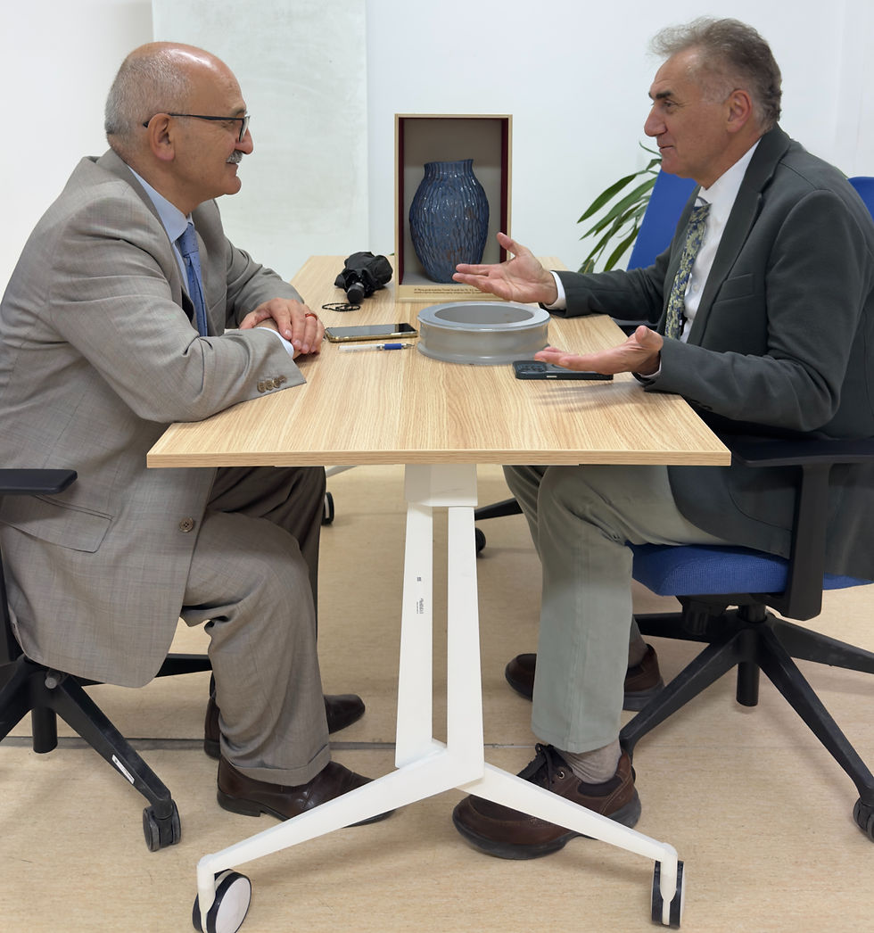
Prof. Dr. Servet Turan, a scientist with international achievements in the fields of materials science, microstructure characterization, and advanced ceramics, was our interview guest in this issue. Turan answered Prof. Dr. İskender Işık's questions on topics ranging from his academic background to advanced ceramic technologies and the future of the sector.
PROF. DR. İSKENDER IŞIK
The ceramics industry is undergoing a historic transformation from traditional production methods to the production of advanced technology and value-added materials. One of the most important architects of this transformation in Turkiye, with his international work in materials science, microstructure characterization, and advanced ceramics, is undoubtedly Prof. Dr. Servet Turan.

Having started his academic journey at Cambridge University, Prof. Turan continues it with the STAR Research Group he founded at Eskişehir Technical University and with national/international projects; he plays a pioneering role not only in academia but also in the integration of electron microscopy and ceramic technologies into industry.
In this issue of our journal, we discussed many important topics with Prof. Dr. Servet Turan, ranging from the frontiers of materials science to the future of university-industry collaboration, from sustainable ceramic production to advice for young researchers. We hope you will enjoy reading this inspiring interview about the past, present, and future of advanced ceramic technologies.
How has your journey in the field of ceramics and materials science unfolded from your PhD years at Cambridge University to the present?
After graduating from Istanbul Technical University's Department of Metallurgical Engineering, I completed my master's degree in engineering ceramics at the University of Leeds as a Ministry of National Education scholarship recipient under Law No. 1416, accepted in 1928. My master's thesis was one of the first to experiment with zirconia, a dental ceramic widely used today, as a dental ceramic.
After learning about ceramics, I decided to pursue my doctoral studies at Cambridge University, then one of the world's leading microscopy centers, to work on the use of electron microscopy in ceramics. This was one of the few courses I failed or had to retake during my undergraduate studies (I didn't get 100 in every course), and I considered it my weak area.
I focused on the characterization of ceramic composite materials using high-resolution transmission electron microscopy. Unraveling the microstructural mysteries of materials at the atomic level allowed me to grasp the tetrahedral relationship of "structure-property-process-performance" to its fullest extent. After completing my PhD, I also worked on welding ceramics using a fascinating technique called capacitor discharge. Following my research experience at three different levels in the UK, I wanted to bring this advanced ceramic knowledge and microscopy vision to my country. As a Ministry of National Education scholarship recipient, I had three choices for appointment, and I listed Anadolu University as my first choice, as it was considered one of the leading universities in the field of ceramics at that time. The most interesting thing is that I had never been to Eskişehir before in my life. So, the university name or the city wasn't important; I chose the one that provided the opportunities and the right scientific environment. I am still very happy to be back in my country and with my university choice.

After being appointed as an assistant professor in the Ceramic Engineering Department at Anadolu University, since all my work required the intensive use of advanced electron microscopes, and because there weren't many microscopes in our country, I continued to work on projects by spending a month in January and 2-3 months at the end of June in England, either with scholarships or my own resources, after teaching my courses during the semester. I became an associate professor in 1999 and a full professor in 2004. Of course, during this time, I had the opportunity to work on numerous different projects. Among these, I served as a project leader or researcher in many projects in the field of ceramics, ranging from plaster to aerospace ceramics. On the other hand, after the establishment of the Ceramic Research Center (SAM) in 1998, our relations with industry increased, and we began to conduct many of our research projects in collaboration with industrial organizations. During that time, together with three professors from our department, we founded MDA Advanced Technology Ceramics, the first company in ATAP, the Eskişehir Technopark.
I served as deputy head of department and deputy director of institute, and organized conferences. In 2004, I became the Founding Director of the Advanced Technologies Research Center (ITAM). In 2006, I headed the Department of Nanotechnology Master's Program, the first of its kind in Turkiye. Two assistants were assigned to ITAM, and for the first and perhaps last time, a supervisor was appointed through a competitive examination. One of the most significant achievements from this period, in my memory, was the establishment of four world-class laboratory infrastructures in the fields of nanotechnology and biotechnology, along with the preparation of an equipment catalog. In 2007, I was appointed Head of the Department of Materials Science and Engineering, and I served as department head during the two five-year accreditation processes with MUDEK (Turkish National Accreditation Board). Through these efforts, conducted with my students and fellow academics, I received numerous national and international scientific awards, including the TUBITAK Incentive Award.

During this period, the concept of priority areas began to take shape. This meant setting aside the subjects you had previously worked on and specialized in, and focusing on different topics in line with the country's vision. Back then, while my colleagues were trying to convince me to become department head for a second time, I said, "Because I'm the administrator, I can't apply to and hire as many scholarship recipients for TUBITAK and similar projects as you do. Therefore, if there are assistant appointments in the department, I'll be their advisor." At that time, we weren't hiring many assistants because we were getting assistants from other universities, and my colleagues accepted my condition. Luckily, two OYP assistants were assigned to the department that period… I wanted to use these assistants to bring new areas to the department and have them work in priority areas. After giving my presentation at the MRS conference, one of the largest conferences in our field, I went around the corridors looking for the most popular topics. While most of the halls had very few participants, one hall was full, and there were scientists waiting in the corridor to fill the seats of those leaving. I waited in line, went inside, and started listening. The topic was solid electrolytes for lithium-ion batteries. After listening for a while, I realized the subject was actually ceramics. Previously, I knew nothing about lithium-ion batteries except their name, so I decided to train one of our research assistants in this field. With the support of our university, we then established the necessary infrastructure. Along with the projects, four doctoral theses and master's theses were completed, which were the first studies of their kind in our country.
Transforming academic theory into industrial benefit has always been one of my top priorities. In line with this, I assumed the roles of Chairman of the Board and R&D Coordinator of the Ceramic Research Center (SAM) in Eskişehir, the heart of Turkiye's ceramics industry. Within SAM, I continue to manage one of the most successful models of university-industry collaboration, overseeing advanced testing, analysis, and product development processes needed by the industry. This journey, which began with atomic-level material research in Cambridge, has today transformed into an ecosystem at Eskişehir Technical University that develops the energy materials of the future, provides direct added value to industry, and, most importantly, trains qualified young engineers, experts, and doctoral students who represent the future of materials science.
What is the biggest shift in mindset or technology you've observed in the field of ceramics science and education in Turkiye over the years?

There have been 3-4 different turning points in the field of education. The first is the introduction of the internet into our lives in the 90s, the second is the pandemic, and the third.
Actually, this event should be considered not just in terms of ceramics science and education, but in a broader sense. When I was doing my PhD in England, to get news from Turkiye, we either had to use video-less phones or go to London and buy certain newspapers that were only sold in certain places, at ten times the price of those in Turkiye, and even then, they weren't daily newspapers, but newspapers from 2-3 days prior. Why did I mention this? Communication in those years was very different from communication in later years. The internet's entry into our lives in the mid-nineties changed many things, including education. Before the internet, to receive science and education, you had to meet with top-level professors and scientists at top universities and in private libraries. In other words, the source of information was limited, but after the internet entered our lives, we became able to obtain much information much more easily online.
In the 1990s, before the internet, to get your project work published in a journal, you would send it by mail in an envelope, and you had no idea if it had arrived, when it would be accepted, or what kind of changes would be requested. You would be notified of the result by mail, which of course took a long time, and then you would make the corrections and send it to the reviewer again. After the internet, we can now submit our academic work for publication with a single click. The internet has changed many things, both scientifically and educationally.
The pandemic also showed that classes and meetings could be held online. It led to a much greater integration of digital technologies into education. Lectures, assignments, and exams changed. It even enabled the development of hybrid learning systems. For example, for the past two semesters, I have been teaching two microscopy courses online, jointly offered by 12 technical universities in our country and taken by students from different universities. This allows us to shorten theoretical lecture hours and increase skills-developing courses without reducing the total number of lecture hours. We need to make good use of this process.
Then, as a result of years of ongoing research, artificial intelligence entered our lives very rapidly. AI can do wonderful things in education, science, and technology, but we also see that a significant amount of the information it provides is incorrect or very incomplete. Therefore, just as a good university infrastructure was necessary for science and education before the internet, now and in the future, teaching staff have once again become crucial in ensuring that we are equipped with accurate information by analyzing much of the information we receive from AI. Furthermore, receiving education in departments with excellent laboratory and technological infrastructure has become important for putting acquired knowledge into practice.
The transformation in ceramic technology has shifted from traditional handcraft and imitative production approaches to an awareness of advanced technology, digitalization, sustainability, and value-added functional/ structural ceramics. Previously, the sector meticulously followed recipes from abroad, gradually developing its own recipes while still following trends. However, in recent years, with the increase in R&D centers, a vision has emerged that prioritizes the production of cutting-edge technologies and charts its own technological roadmap. The production approach has moved beyond aesthetics and capacity, evolving towards ecosystem design focused on carbon footprint reduction, energy and water efficiency, and recycling. In addition to clay shaping and classic mold systems, 3D ceramic printers, digital ink systems, large-format porcelain slab production, and automation have become widespread in the design and production phases. Research in areas such as laser and microwave sintering and functional surface development, along with the establishment of pioneering R&D centers, has advanced our technological development to a higher level.
Advanced Ceramics and Nanotechnology
When comparing traditional ceramics with structural/ functional advanced technology ceramics, where does the Turkish industry currently stand in this transformation?
Before answering this question, it is necessary to provide some information. While our country is a global giant in traditional ceramics such as tiles, vitrified products, tableware, and earthenware, it exhibits a highly dependent profile on foreign sources in structural and functional technical ceramics used in the aerospace, defense, electronics, biomedical, and machinery industries. Turkiye is one of the strongest players in the world and Europe in traditional ceramic production, and ranks 2nd in Europe and among the top 10 in the world in ceramic coating materials production. It is also the largest producer and exporter of ceramic sanitary ware in Europe.
Currently, the volume of high-tech ceramics produced is far less than in previous years, while the capacity of traditional ceramics has increased significantly. We continue to import many high-tech ceramics from abroad. Not only high-tech ceramics, but even normal traditional ceramics are still imported and sold in our country despite there being no need for them. The Turkish ceramics industry is still in the early stages of the transformation between traditional ceramics and structural/ functional high-tech ceramics.
In our country, domestic companies have been established and have started mass production, producing ceramic cutting tools and wear-resistant industrial parts from non-oxide advanced ceramics, holding their own patents. Projects to localize the production of advanced armor ceramics, such as boron carbide and titanium diboride, from raw materials to final products, are the biggest financial and strategic engine of this transformation. In addition to companies, mostly founded by academics, producing ceramics such as zirconia, alumina, and geopolymers, ranging from zinc oxide sunscreen to piezoelectric materials and sensors, there are also companies established, particularly in the defense sector, that produce advanced ceramics. Similarly, the future of the sector can be accelerated by transferring the added value obtained from traditional tiles to structural ceramic investments in fields such as defense, electronics, and medical.
What are the turning points you expect to mark the next 10 years in the field of structural ceramics, ultra-high temperature ceramics, or coatings?
Research on structural ceramics has decreased. However, studies on ultra-high temperature ceramics, functional materials, and energy-related materials have been increasing in recent years and continue to do so. The most important of these are sodium-ion batteries, thermoelectric materials, and insulation materials.
Materials Science and Engineering, particularly advanced ceramics, will undergo transformations in the next 10 years centered around extreme resistance to harsh conditions, artificial intelligence integration, and sustainability. Positive turning points include: the production of high-entropy diborides and carbides formed by combining five or more elements; the shaping of UHTCs in complex geometries; breaking the taboo of brittleness in structural ceramics and enabling the use of silicon carbide matrix silicon carbide fiber composites in civil aviation engines; the widespread adoption of self-healing ceramics; the theoretical formulation of different ceramic phase combinations using artificial intelligence and machine learning; and the resolution and mass production of room-temperature ionic conductivity problems for ceramic electrolytes in solid-state batteries.

What are the most exciting projects you are currently focusing on within the STAR research group that you lead?
First, I'd like to explain the meaning of the STAR research group. STAR is actually an abbreviation of the words Servet Turan Research. After us, the TUBITAK intern student project program also adopted the name STAR. But we adopted this name before them. In our group, students and scientists work together at every level, from first-year undergraduate students to professors. Currently, our most exciting projects are those we are working on under a different concept we have developed regarding the use of waste. So, what is this concept? I can explain it like this: Instead of using the word waste, we are now evaluating waste with a different approach, going beyond the circular economy, by evaluating waste according to its industrial processing status. In waste evaluation studies conducted so far, research is carried out by looking at the chemical content of the waste and determining in which areas it can be used. In the concept we are trying to develop, the focus is on identifying and evaluating the new properties acquired by the waste during the process leading up to its formation, and determining its areas of use. In this respect, it differs from the circular economy, industrial symbiosis, and the concept of secondary raw materials that devalue waste.
Within this scope, we are continuing our exciting work on the production of energy materials and ultra-high temperature ceramics from waste, as well as the production of silicon carbide ceramics, one of the important advanced technology ceramics, from waste. In addition to these, ion batteries, thermoelectric materials, and insulation materials are also among the other exciting studies being carried out in our group.
Characterization and Microstructure (Electron Microscopy)
The most critical element determining the performance of ceramic materials is microstructure control. How have developments in electron microscopy changed ceramic development processes?

When I began my first microscopy studies in the 1990s, microscopes could only examine specially prepared, clean, cavity-free, oil-free, and undamaged samples coated with gold or carbon. Chemical analysis and phase analysis were quite limited in microscopes. Therefore, it is necessary to mention some techniques that are now industry standards but did not exist back then, for those familiar with today's technologies.
The 1990s were a period of complete breakthrough and transformation in the microstructure control of ceramic materials, and consequently in electron microscopy, in terms of digitalization, analytical precision, and nano-scale characterization worldwide. Grain boundaries, phase transformations, and crystal defects of advanced ceramics began to be elucidated at the atomic level thanks to technological advancements during this period. For example, while it was necessary to examine ceramics, which are insulating materials, at high resolution at low voltages without the need for coatings, field-emission filaments that would enable this were not available.
Analytical electron microscopes and energy filters that would allow the detection, chemical analysis, and mapping of atomic-scale impurities accumulating at grain boundaries, especially light elements such as boron, nitrogen, oxygen, and carbon, which determine the properties of ceramics, were either absent or limited in number. In my doctoral thesis, which was based on microscopes, there were almost only 2-2 spectra; imagine what other theses were like.
CCD cameras, which allow for the digital analysis of micrographs, did not exist. We used film for images, developed them in a darkroom, and printed them ourselves. Although grain orientation is crucial for the performance of ceramics, Electron Backscatter Diffraction (EBD) technology, whose foundations were laid in the 1970s and which automatically generates grain orientation and phase maps in the microstructure of materials, did not exist. Oh, and let's not forget that the concept of nanotechnology had not yet been introduced.
Back then, there were no focused ion beam-scanning electron microscopy (TEM) combination devices that could model the 3D internal structure of a material and prepare TEM samples by shaving ceramic samples with nanometer precision, obtaining layer-by-layer images, chemical maps, and phase maps, and combining this information in a computer environment. In fact, it turned out that tests of this device were being conducted in a room we weren't allowed to enter at the time.
While classical methods examined ceramic grains as a whole, aberration-corrected scanning transmission electron microscopy technology, which corrected the lens maps necessary for imaging the boundaries where grains meet at the atomic level and performing chemical and phase mapping to determine whether elements were located at grain boundaries or in the crystal lattice, was also developed at Cambridge University during that period.
In situ electron microscopy technology, which could monitor the behavior of materials under extreme conditions in real time within the microscope and instantly record many events such as phase transformations and grain growth, did not yet exist.
But now, with the advancement of technology, we can place all kinds of samples inside the microscope and produce products or nanotechnological products without preparing the samples inside. We can also use highly advanced technologies for chemical analysis, phase analysis, and examining these not only in two dimensions but also in three, and even performing chemical analysis of individual atoms. Here, I would like to mention another important concept: technology and science always follow each other. Developments in science trigger technology, technology develops, and developing technology enables a better understanding of science, and this cycle constantly repeats. We experience this cycle not only in the field of ceramics but in all fields.
Developments in electron microscopy have triggered numerous developments and innovations in the development processes of advanced ceramic materials and in improving functionality in other materials, making nanotechnology possible, etc.
Is the importance of microstructural analysis in root cause analysis of material failures or quality problems in industry sufficiently understood?

In fact, it's not just about microscopes; microstructural characterization should be considered as a whole. We need to understand that effective root problems can only be solved by understanding and combining these techniques effectively. Once this is grasped, the rest becomes much easier. Many businesses, when a piece breaks, is manufactured incorrectly, or is damaged, opt for superficial and temporary solutions instead of investigating the deep microscopic causes behind the problem. Microstructure is the most important element in materials, showing us the genetic historical map of a material's production history and the conditions it has been exposed to. Microstructural analysis, one of the most effective methods used in problem-solving, should not be a luxury, but the first and most essential step in root cause analysis.
In this context, electron microscopes and x-ray diffraction meters are available in almost every province of our country for problem solving, provided we don't shy away from understanding the problem and the extremely low equipment usage costs compared to our losses. While we're on the subject, I'd like to mention one more thing: our companies invest heavily in characterization equipment, and many of them become unusable shortly after due to lack of maintenance or expertise. Instead, entering into agreements with those who own the equipment to obtain their services could be considered an important step. Of course, this applies to equipment they use only once a day or once a week.
University-Industry Collaboration and the Turkish Ceramics Sector
Turkiye is a significant force in the world in traditional ceramics (tiles, vitrified ceramics) production. However, how can academy-industry collaboration be made more efficient in the transition to high value-added advanced ceramics production?

Unfortunately, academy- industry collaboration is quite weak in every sector. The main reason for this is the lack of empathy between the two sides. Numerous mechanisms to bring academia and industry together have been put into operation recently, but despite this, it is still not at the desired level. On the other hand, the most important point in advanced ceramics production is that our country's consumption in this field is not high. Therefore, since large companies do not invest in such areas, many academic studies conducted at universities do not turn into investments. Generally, inventors try to turn their inventions into investments by establishing technopark companies with limited financial resources, and the company remains small. This creates a significant cost disadvantage against companies producing high volumes of products in other countries, preventing the company from growing. The companies that grow in this field are generally those that produce materials that are not allowed to be imported from abroad.
Let's focus on what needs to be done structurally, financially, and culturally to encompass all sectors, but first, let's talk about the existing opportunities. Currently, the Ceramic Research Center, which operates on a shared infrastructure model, focused clusters and centers of excellence, and technology transfer offices that only handle bureaucratic processes between universities and industry, exist in our country as university- industry collaboration mechanisms. Advanced equipment necessary for material production and characterization is very costly; not only is its acquisition expensive, but its sustainability is even more costly. Shared laboratory infrastructures, such as the Ceramic Research Center (SAM), where academia and industry can use it jointly and share costs, should be supported and developed. One of the biggest bottlenecks between universities and industrial organizations is the sharing of patent rights. Flexible and fast standard contract models should be developed that are based on the "win-win" principle and prior knowledge ownership, that will not discourage the industrialist's appetite for commercialization, and that will reward the academician with copyrights. Most projects are shelved due to disagreements over patent rights.
What is our current situation regarding the transformation of our domestic raw material and ore processing potential in the ceramics sector into advanced ceramic powders?
Despite being one of Europe's largest producers of traditional ceramics and possessing rich reserves of feldspar, clay, and quartz, and more importantly, the richest boron resources, Turkiye is still in its infancy in transforming these raw materials into advanced ceramic powders used in fields such as aviation, defense, and electronics, and remains largely dependent on imports. Regarding your previous question, the production of advanced ceramics is not very high either in our country or globally. This is actually one of the parameters that most significantly affects powder production.
Turkiye's most advantageous area is boron compounds. Recently, a company was established in our country to produce boron carbide powder, and it is currently in operation. The technical ceramics sector in Turkiye has shown growth in recent years. However, our companies generally import the powder and choose to shape and sinter it in Turkiye. Although some institutions have successfully conducted academic studies on producing advanced ceramic powders from domestic raw materials, this process has not yet transformed into a large-scale commercial raw material industry. The main reason for this is the small scale of use and production, and the lack of exports. Incentive mechanisms are available for the production of other powders, and investors are being sought.
Future Projections and Advice for Young Researchers

All kinds of materials are the embodiment of developments in the world. For example, all innovations in medicine, aviation, and computer technologies require materials technologies to touch human lives. In other words, material production will continue as long as the world exists. However, metal production may decrease, especially in metals, which are the most recyclable material group. However, alloy production will not decrease due to recycling. Considering that many professions are expected to disappear with the development of artificial intelligence, materials science and engineering will always be needed. Therefore, I strongly recommend materials science and engineering to young researchers.
I previously published a letter of advice online in response to similar questions from students, titled "What would I do if I were a student?", which became quite popular. Of course, much has changed since then. Now, when I think about what I can say, it's critically important for young researchers, who will shape the world of the future, to adapt to the rapidly changing scientific and technological ecosystem. In this new era, where artificial intelligence, data science, and interdisciplinary studies are prominent, taking strategic steps is necessary to build a successful academic and professional career. Thanks to the internet, information has become very easily accessible, and with artificial intelligence, there's no need to filter and combine information; we can get direct answers to our questions. But transforming this information into a product will always require technical skills. Therefore, developing laboratory techniques and manual dexterity, being able to read data, and filtering information will become important skills.
Don't limit yourself to reading publications and attending conferences in your own field. Explore methodologies from different disciplines to make a difference. Build a strong network and use social media academically: actively use platforms like LinkedIn and ResearchGate to follow global researchers, participate in current debates, and publicize your work. Attend conferences, but not just to give presentations; seize opportunities to meet people at poster sessions, exchange ideas during coffee breaks, and find potential partners. Connect with multidisciplinary laboratories. Don't be discouraged by rejected articles, negative peer reviews, and failed experiments; use feedback to improve yourself without taking it personally. Never compromise on ethical principles; scientific ethics and academic integrity will always be crucial for your long-term reputation. Some things happen late, sometimes with difficulty, and everything can be put back together, but once reputation is lost, it never returns.
On the other hand, we mentioned that materials science and engineering are among the most strategic fields that will exist in the world of the future, from green transformation to the defense industry, from the semiconductor crisis to biomedical technologies. Future projections and career advice specific to our profession in this field could be as follows: In terms of knowledge, focus on materials informatics, sustainability and circular economy, smart and functional materials, and energy and health-related materials. In terms of skills, learn computational materials science tools, specialize in characterization techniques; correctly analyzing the micro and nano structure of a material is as critical as producing it. Don't just be an operator of advanced characterization instruments like SEM, XRD, TEM, XPS, and AFM; thoroughly understand the physical and chemical theory behind them. A materials engineer who correctly interprets data and filters information accurately will always be highly valued.
How will the Green Deal, carbon neutrality targets, and sustainability principles affect ceramic material technologies and material choices?
In fact, all three concepts focus on material technologies; reducing energy consumption and using resources efficiently are paramount in ceramic, polymer, and metal production to achieve carbon targets.
The European Green Deal, carbon neutrality targets, and sustainability principles necessitate a radical transformation in the ceramics sector, which consumes high amounts of energy and raw materials. These global policies will fundamentally change ceramic production technologies and material choices, forcing the sector towards a more circular and low-carbon structure.
Ceramic production, particularly during the firing phase, requires very high temperatures and therefore consumes significant amounts of fossil fuels. Carbon neutrality targets directly impact these processes. Traditional natural gas kilns will be replaced by green hydrogen, biomass fuels, and electric/hybrid kiln technologies, some companies have already begun using such methods. Technologies related to electricity generation, storage, and hydrogen conversion from solar energy will gain importance. Reusing waste heat from kilns for sludge drying or plant heating will become standard practice. Optimizing kilns and ensuring error-free production processes will reduce waste rates, minimizing energy and raw material waste.
The use of innovative minerals and additives that lower firing temperatures will increase. The use of industrial glass waste, fired ceramic waste, iron and steel and mining waste, and fly ash in recipes—in other words, the circular economy model—is being encouraged. However, the industrially processed raw material model, which I mentioned in the answers to previous questions and which we proposed, will surpass even the circular economy model. To reduce material consumption and logistics, for example, the thickness of porcelain tiles has been reduced to 3-5 mm. Carbon border taxes and pressure to reduce logistics-related emissions are forcing manufacturers to source key raw materials such as clay and feldspar locally instead of importing them from distant countries. On the other hand, ceramic preparation processes consume a lot of water. New technologies are making it mandatory to use nearly 100% closed-loop water recovery systems in production.
The ceramic factories of the future will be facilities powered by green hydrogen, digitally optimized, using circular raw materials, and exempt from carbon taxes. The Green Deal, carbon targets, and sustainability will positively influence ceramic production technologies and material choices. Traditional ceramic production processes come to mind as a sector where waste generated in many sectors can be utilized. In this context, I define traditional ceramics and the cement sector as sectors that can recycle. It is important to make a distinction here: recycle is one thing, while the sustainable is more valuable and a different concept altogether.
What specific areas would you recommend young researchers and students who want to pursue careers in ceramics and materials science and engineering to focus on?
Materials science and engineering, including ceramics, is a very broad and rapidly evolving field. But returning to the previous question, the green agreement, carbon targets, and sustainability, along with the circular economy, are making sustainability and energy materials particularly valuable.
On the other hand, the most strategic specific areas that young researchers and students can focus on might be: Energy materials and storage technologies, ultra-high temperature ceramics, ceramic matrix composites, bioceramics and health technologies, electronics, optics and quantum materials, semiconductors, photonic crystals and optical ceramics, digitalization and AI-assisted material discovery, material design with machine learning, additive manufacturing and innovative green manufacturing processes such as cold sintering, which reduces the carbon footprint during production and enables firing at lower temperatures.
Finally, how are the preparations for the SERES Congress progressing?
The International Congress on Ceramics, Glass, Enamel, Glaze, and Pigments will be held in Eskişehir for the 6th time. Our congress was somewhat disrupted during the pandemic, but as one of our association's important events, we want to revive the SERES congress and create a beneficial meeting point for the ceramics ecosystem. Preparations are proceeding rapidly and intensively as planned. We always encounter setbacks in such large organizations, but we continue by solving the problems. A 3-day program has been created that will address our previous problems and will include topics related to ceramic art and traditional ceramics, as well as all stakeholders in the field of ceramics, focusing on what are defined as the technologies of the future.

This congress, organized jointly by two universities in Eskişehir across two different campuses and in collaboration with the Turkish Ceramics Society and the Turkish Ceramics Federation, will feature presentations by four international scientists, each lasting forty-five minutes, that will help us chart a future vision. In addition, there will be over 30 invited speakers addressing important topics. Approximately 100 oral presentations, around 35 posters, 2 exhibitions, and 5 workshops will also be presented. The congress, which will see participation from the ceramics sector and universities, will also include two panels on sustainability and ceramics R&D centers. Venue provision and sponsorships are crucial for such large-scale events; I would like to express my sincere gratitude to the rectors of Eskişehir Technical University and Anadolu University for their support. Without the financial support of our 26 sponsors, it would not have been possible to hold this congress in its current form. In this context, I wholeheartedly thank all our sponsors.


Yorumlar